The researchers at the Institute of Technical Physics and Materials Science of the ELKH Centre for Energy Research (EK-CER) are developing advanced semiconductor materials and technologies with a strong emphasis on energy efficiency and sustainability within an ongoing Thematic Program of Excellence. These materials and processes can be utilized for manufacturing more efficient light sources (LED) and electronic devices, and for catalysizing the production of hydrogen from water.
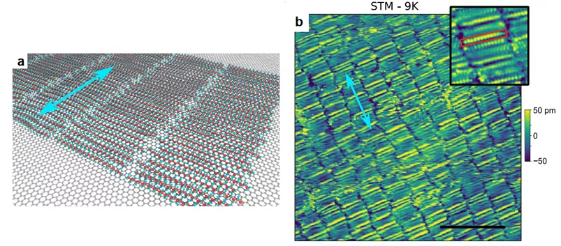
Structural model (a) and atomic resolution STM image (b) of a self-assembled molecular layer composed of 20-26 carbon atom alkane chain, formed on the surface of graphene
Semiconductor materials are of fundamental importance in numerous areas of the industry, particularly in those of digitalization. Semiconductor devices serve as the foundation for digital electronic devices, efficient light sources (LED), and a wide range of sensors. The novel 2D and 3D nanostructures created by EK-CER researchers can bring significant advancements in these fields and enable the development of more efficient, faster, and lower-energy utilization semiconductor devices in the long run.
2D heterostructures, known as artificial crystals, constructed atomic layer by atomic layer from 2D crystals, form a new family of materials whose structure can be controlled to an unprecedented extent, compared to other substances. Observing and interpreting the novel physical phenomena that emerge in these materials enables the targeted production of new materials with planned electrical, optical, or magnetic properties. The researchers at the institute became the first in the world to observe, using scanning tunneling microscopy (STM) measurements, the self-organized molecular layer structure and composition formed on the surface of various 2D crystals, including the semiconductor molybdenum disulfide (MoS2), at atomic resolution. The results facilitate the improvement of operational stability for devices based on semiconductor 2D crystals under real-world conditions.
Additionally, the researchers have developed a straightforward method based on sputtering for producing homogeneous and thin MoS2. By depositing 2D MoS2 (p+) onto a monocrystalline semiconductor, intentionally heavily doped silicon carbide (SiC) (n+), Esaki diode characteristics were successfully measured. Due to their negative differential resistance, these can be used in devices suitable for amplification. The results provide a better understanding and enable the precise design of devices based on 2D crystals, as well as the technical solutions for creating small-sized, low-material-consumption, and low-energy-demand electronic devices.
EK-CER researchers have made progress in the catalysis of hydrogen production from water, which holds promise for truly green hydrogen generation. They have been working on the development of new and cost-effective nanoscale catalysts that enhance the efficiency of photoelectrochemical water splitting by introducing a co-catalyst that improves interfacial reaction capability on a semiconductor. For this purpose, a simple, iron-containing compound was employed on a 3D nanopyramidal structure bismuth vanadate (BiVO4) semiconductor. The objective of this development is to enhance the efficiency of energy storage methods that come to the forefront with the proliferation of solar panels.
The project (TKP2021-NKTA-05) is being carried out until the end of 2025 with the support of the National Research, Development, and Innovation Fund of the Hungarian Ministry of Culture and Innovation. The funding is provided through the TKP2021 grant program.